Teardown of the IKEA ROTHULT RFID lock
EDIT: You can connect an stlink to the debug header. I never got that far in the writeup though, due to this being the first ARM project I looked at combined with the vacation ending. I have however tested it and it works.
Disclaimer: If you believe any of the below and burn down your house, lose your dog, or break your lock, or something else that is good or bad happens, it is your own fault. The likelihood of something being wrong is close to 100%.
The IKEA ROTHULT is an RFID-enabled motorized lock for desks, cupboards, etc.
Obviously, it would be nice if it could be connected to, for example, a mysensors network and used for home automation.
Teardown
The ROTHULT is kept together by four screws, no tricky plastic tabs. Simply unscrew the battery compartment and the lid, then lift it away.


Inside, you find the bolt, a gearbox arrangement with a small motor, and a circuit board. The RFID antenna is beneath a snap-in lid (visible in the first picture) and connected through four pins to the PCB. Two microswitches are used as end stops for the bolt.

Unfortunately, the RFID antenna is soldered to the main PCB, which means that it cannot be lifted out of the box easily. Everything else can be removed without violence.


To remove the lid over the RFID antenna, lift CAREFULLY at the slots, while pushing the plastic tabs from the inside.

If you don’t manage to push ”good enough” on the tabs, they are likely to break. (The two closest to the PCB on mine did, but it doesn’t really matter, if you are to use the lock as a lock later, it will not be visible and super glue is cheap :-) )
Lifting the lid reveals a PCB with an antenna on it. Unfortunately, that is all it seems to be, there is no hidden I2C/SPI/serial RFID module ready to be harvested.


PCB
Let’s take a closer look at the PCB.
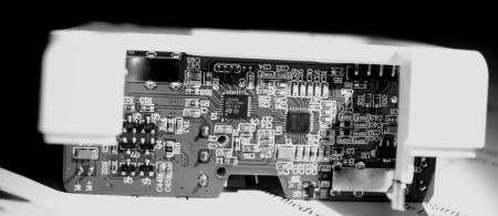
Q3-Q8 on top to the right seems to be the power transistors driving the motor.
The build is primarily surface-mounted (no surprise), and uses two main integrated circuits – a guess is that the right one handle the RFID decoding, and the left is the main processor (if there is such a thing in this device). Then, if we are lucky, the header right above the integrated circuit could be a programming/debug header.
Processor

A closer look on the suspected CPU reveals the ST logo, and an identification number: L051K86, which is a reasonable match to the STM32L051K8 processor with LQFP32 pinout (datasheet).
If this indeed is the case, the pinout from the datasheet is shown below, rotated to match the photo above.

Looking at the header (ref black-and-white photo), from left (H1) to right (H6), the header pins appear to be connected as below – please note, this is still to be confirmed by a second view as well as with measurements!
- H1 – Pin 24 (PA14, SWCLK, USART2_TX)
- H2 – Pin 23 (PA13, SWDIO)
- H3 – Pin 17 (VDD)
- H4 – PCB ground plane (if one look at the battery compartment, the negative pole of is connected to the same PCB plane)
- H5 – Pin 20 (PA10, USART1_RX)
- H6 – Pin 19 (PA9, MCO, USART1_TX)
According to the datasheet (section 3.9 boot modes), programming the flash memory is done by using SPI1 (PA4-PA7), SPI2 (PB12-PB15), USART1 (PA9, PA10), or USART2 (PA2, PA3).
Since we indeed have USART1 connected to H5-H6 is would seem as if we can access the flash through this header (if the BOOT0 pin can be manipulated / is connected in an appropriate way). The datasheet in turn refers to STM32 memory boot mode AN2606. That datasheet can be found here.
For the remaining pins, H1/H2 are connected to the serial wire debug feature (SWCLK, SWDIO), see for example this datasheet for more details.
Let’s leave it at this for now, and move on to the rest of the circuitry.
RFID Decoder
The initial assumption is that integrated circuit #2 is a dedicated RFID decoder.

This is confirmed by a new macro photo (the print on this circuit is really hard to read) which identifies it as an AS3911 (datasheet) NFC Initiator / HF reader IC.
The ams logo is quite identifiable once you know it is supposed to be there.
Looking in the datasheet, we find the pinout:
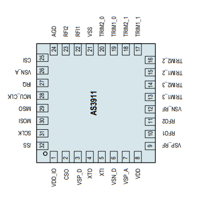
Again, his is oriented the same direction as in the overview PCB photo (but not as in the closeup showing the markings) and the connections to the CPU can be traced:
- AS3911 Pin 32 (/SS) <-> CPU Pin 10 (SPI1_NSS)
- AS3911 Pin 31 (SCLK) <-> CPU Pin 11 (SPI1_SCLK)
- AS3911 Pin 30 (MOSI) <-> CPU Pin 13 (SPI1_MOSI)
- AS3911 Pin 29 (MISO) <-> CPU Pin 12 (SPI1_MISO)
- AS3911 Pin 27 (IRQ) <-> CPU Pin 14 (PB0)
Hence, the AS3911 is connected to the CPU through SPI.
End Switches
The two microswitches seems to switch VDD/GND to an IO pin depending on their position.
- Switch 1 (above the summer) is connected to CPU pin 27 (PB4)
- Switch 2 (not above the summer :-)) is connected to CPU pin 28 (PB5)
Summer
No idea.
Motor Drivers
Not investigated yet.
Continued in part 2, where we wire up the debug header and decode the serial output.

Lämna en kommentar